
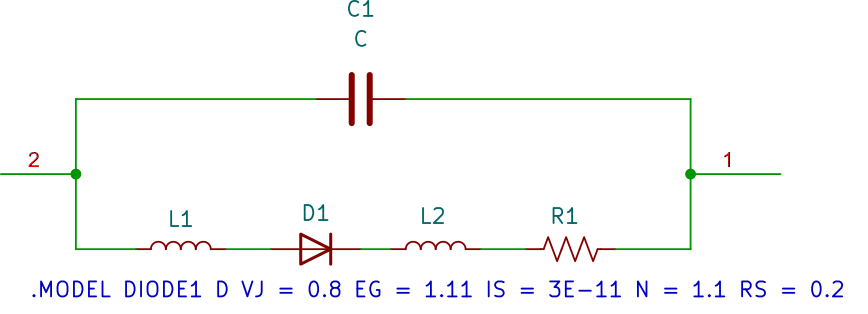
For simulation purpose a laser diode can be modeled by the subcircuit shown below. The circuit elements represent the unwanted parasitic inductance, capacitance, and resistance which exist in the laser diode module. The inductance is mainly from electrical connections and vary depending on the technology using, wire bonding, ribbon bonding or strip lines have reducing inductance order. The diode model can be adjusted to give the laser diode forward voltage drop. The junction capacitance dominates the capacitance. We expect a larger capacitance for a large high power laser diode than for a small low power laser diode. For most laser diodes the model that can be downloaded below if sufficient or exploring the behavior in a circuit. For closer match to the performance of a particular laser diode the inductance, capacitance, and diode drop can be obtained from the supplier. Alternatively the model values can be fitted so simulation match a measured pulse response.
L2 3 5 0.5nH
D1 1 5 DIODE1
C1 4 2 1pF
R1 4 3 0.1R
L1 1 2 0.5nH
Figure 1. Laser diode simulation model.
For many laser diodes the inductance L1 and L2 will take a larger value. Here the interest was to explore the potential of the driver design in a best case scenario.
| Description | File name | Download |
|---|---|---|
| SPICE simulation model for laser diode | LDeq_SPICE.zip | Download |