
A biased photodiode is a good optical probe. The input amplifier of an oscilloscope allow detection of mV signal. For detection with an analog to digital converter or in case of very low signal levels a preamplified PD signal is needed. This project is for a trans impedance photodiode amplifier (TIA).
The circuit is based on the OPA380 Precision, High-Speed Transimpedance Amplifier.

The aim with the circuit is to get a 0V to 3V output for no light to max light incident on the photo diode. To get good linearity down to no light it is necessary to have a negative supply rail. In the simulation it is the -5V supply. The pull down resistor R3 to -5V on the OPAMP output is a trick suggested in the OPA380 datasheet to improve performance around 0V.

Simulation results for 0A to 50uA is shown in fig. 2. The graph show a good temporal response that returns to 0V when the current is 0A. The gain resistor R2 is 47kohm. With 50uA current we expect Vout = 50uA * 47K = 2.35V. We see that the max voltage is only 1.17V. That is because of the 47R series resistor R4 and the R5 termination resistor, which gives a divide by 2 voltage divider. The series resistor will be on the PCB while R5 represent an external 50ohm termination. This setup is preferred for measurement of time varying signals. With a slow detector like ADC it is suggested to use a hold capacitor and 1K termination. The gain resistor R2 can be selected for the desired gain. Higher gain gives less bandwidth. The circuit can be used up to 470k gain provided that the OPAMP does not saturate.
All in all the simulation results show that the circuit is a good basis for our PCB design.
PCB design
We want some extra features on the PCB. The circuit uses a negative supply rail. to avoid having to supply the PCB with both a negative and positive the negative supply is generated on the PCB. A good solution for the inverter is a High-Frequency, Regulated, 200mA, Inverting Charge Pump IC, the MAX889. Compared to an inductor based inverter circuit the charge pump gives less noise coupling from the switching.
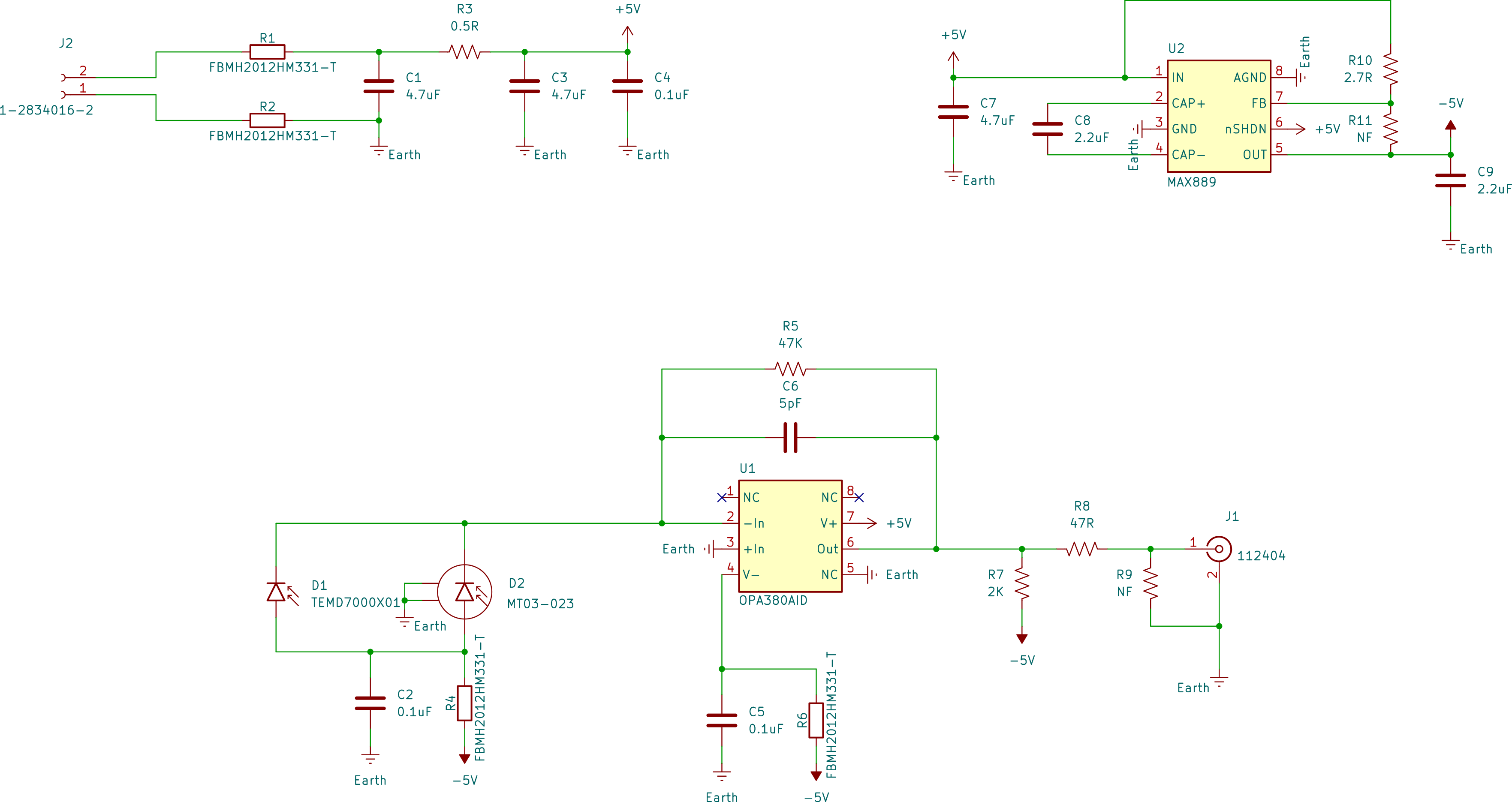
The two photodiodes D1 and D2 in the schematic in fig. 3 are for alternative footprints, one 0805 surface mount PD and the other for TO-can 3 or 2 pin through hole package.
The negative supply is distributed through R4, R6 and R7. This gives some population options for optimizing for sensitivity or speed. With R4 fitted the photodiode has reverse bias which improves speed but as a side effect increase dark current. For smallest possible resolvable optical power it is better to leave R4 non-fitted (NF) and populate C2 with a 0 ohm resistor. With the PD will operate without bias. With R6 fitted the OPAMP has + and – supply and R7 should not be strictly necessary. Still R7 insures that the zero level is a driven level so it gives the best performance for measuring near zero power. There are many photodiode trans impedance circuits proposed in the literature and technical notes. This is probably the best for most amplified PD use cases.

The board layout is shown in fig. 4. It uses 0805 case passives and 8SOIC IC’s. The design is intended for mounting on an M4 mounting bracket that fits atop a standard optics post.


The KiCad project and design files are share as open source hardware.
Feel free to download explore and fabricate or modify to tailor for your applications.
| Description | File name | Download |
|---|---|---|
| KiCad Project, open with unarchive project | Amplified_PD.zip | Download |
| Gerber files and BOM ready for fabrication | Amplified_PD_KiCad_production_files.zip | Download |
| SPICE simulation schematics and models | Amplified_PD_SPICEsim.zip | Download |