
Introduction
This project is for a laser diode driver that can drive constant current through a laser diode. The current control is fast settling (<10ns) so it can be used for pulsing or arbitrary waveforms. The control is via SMA coaxial 50Ω connector input. An added DC offset is set with the onboard trimmer potentiometer. The laser diode connection is by soldering to the universal footprint that will accommodate TO-can through hole lasers or butterfly packaged lasers. This article describes the workflow and considerations that lead to the final PCB design. The KiCad project can be downloaded below. It can serve as a starting point for your own tailored design or used directly by fabricating the PCB.
The driver can run diode lasers in CW operation for example for optical pumping of active fibers. The main feature of the drive is its capability to modulate the laser current with quick response times. There are commercial seed drivers or analog drivers on the market. These are aiming for very fast rise time, often faster than what an actual laser diode will follow. This design is based on low cost general purpose components the make a more accessible solution fully adequate in most applications. The spirit of the site is to give electronics skills the optics people and demystify optoelectronics for electronics people. Which ever angle you come from going through the project will add more than pushing through the 1k dollar purchase order for a commercial driver. Here are some examples of laser diodes that are obvious to drive with a driver like the one we are working on. We have to look at the mechanics of the laser modules and the electrical driver requirements.


| Pin | Connection |
|---|---|
| 1 | TE Cooler (+) |
| 2 | Thermistor |
| 3 | PD Anode (-) |
| 4 | PD Cathode (+) |
| 5 | Thermistor |
| 6 to 9 | NC |
| 10 | LD Anode (+) |
| 11 | LD Cathode (-) |
| 12 to 13 | NC |
| 14 | TE Cooler (-) |
Figure 2. 14-pin butterfly package and pinout.
Package / Case are for most intents synonymous. The pin table indicates that the package contain more than just the laser diode. The TE Cooler is a thermoelectric l cooler, a Peltier element that cools when current is flowing + to – and heats when the current is reversed. A thermistor pin 2 to 5 is also integrated to enable closed loop temperature control. The temperature changes and required TE currents are slowly varying and connections can be wired without loss of performance. There are some commercial TEC drivers offered on the market. Most are pulse width modulated, which can couple noise the the laser current. I have a project in the pipeline for an analog, non-switching TEC driver. The PD is a back facet power monitor photodiode. It can be reversed biased and used for monitoring the temporal behavior of the laser power. The bandwidth is typically not high enough for real temporal analysis. In this project we will only use the LD Anode (+) on pin 10 and LD Cathode (-) on pin 11.

The power vs. operating current show a threshold current of 60mA, where after the power increases linearly with the current. That is why we can expect that modulation of the current gives a proportional modulation of the optical power. It will be practical if the driver allows setting of a DC bias equal to the laser threshold, so the modulation acts on the linear range of the current to power curve. The power vs. current characteristic is going to be similar for all laser diodes. The forward voltage is < 3V for this 633 nm laser. The laser diode forward voltage is largely determined by the band gap energy, which is why voltage tends to be inversely related to wavelength. Typically, the voltage for red and infrared wavelength diodes is between 1.5V and 3V but for green, blue, and ultraviolet above 5V. This sets some electrical boundary conditions for our driver development. We want the driver to work with as many types of diode lasers as possible.
Regarding the mechanics this 14 pin butterfly package is common for fiber coupled lasers. For free space coupling TO-can module are more common, particularly in the low <0.5W average power range. The figure show a TO-56 Package pulsed laser diode.
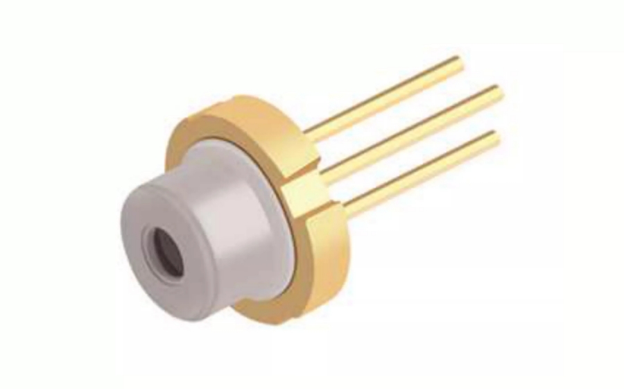
The so called pulsed laser is designed for low duty cycle, high peak power pulses with long off time in between. The limitation is mainly the maximum power dissipation. The specification of the example pulsed laser diode is max tp = 100 ns and f = 1 kHz, 100ns/1ms is 1E-5 = 0.001% duty cycle. The peak power and current translates to averages values of 6.5mW and 2mA, that is a good efficiency. We have a good short pulse laser diode driver in the project. The aim for this project is driver laser diodes in CW to pulsed. The current range is mA to 1A .

The simplified schematic proposes a constant current circuit for the driver. Let's see how it works. The resistor R works as a current sensor. It can be a low value (<1Ω) sensing resistor. The operational amplifier U compare the current sensing signal on the - input with a current set-point IN on the + input. If the + input voltage is larger than the - input the OPAMP output will swing positive. With a higher gate voltage on Q the current through the LD which flow through R will increase and the – input voltage go up. Similarly, but opposite if the - input is above the + input. In this way the feedback will act until the current through R gives a voltage drop equal to the set point IN. Notice that we only require the transistor Q to pass a current that increase when the gate voltage increases. Any n-type MOSFET or BJT will act like that. There are commercial drivers for modulation of laser diode based on this simplified schematic that uses high speed RF transistors. These drivers can potentially give current rise times of <1ns. My experience is that with most relevant laser diodes with more than 50mW output power the laser diode is limiting the rise time. As discussed in the short pulse driver project the LD has parasitic capacitance and induction that work as a low pass filter. In the spirit of this site, we will use a cheap MOSFET and see what kind of modulation is possible.
In a parametric search on supplier site (e.g. DigiKey) I look for Vgs(th) well below 5V so we can use 5V supply voltage for the OPAMP. To get high speed a criterion is low Gate Charge. For switching the MOSFET the gate has to be charged and discharged. The OPAMP has limited drive current, so a low required charge is important. To drive 1A laser diode current we need some power handling of the MOSFET. The max current, Continuous Drain (Id) is specified for the fully on transistor, where it takes its Ron resistance. In the constant current circuit the MOSFET is regulating, so it can not be fully switched. For that reason we need to over upscale the power handling and max current. An overall good candidate seems to be the onsemi FDD1600N10ALZ in TO-252-3 (DPAK). This DPAK case has good Power Dissipation, 14.9W max. I was also glancing to the max Drain to Source Voltage (Vdss). If a laser diode has high capacitance and inductance it is possible to increase speed by increasing the laser diode voltage. With 100V Vdds we have some room for experimentation. Note that rise time is not a searchable parameter for such general purpose transistors. We used the gate charge as an indirect parameter. The datasheet of the FDD1600N10ALZ does specify rise and fall time of 2ns. That looks promising.
The OPAMP needs to keep up. Slew Rate, Current - Output and 3db Bandwidth are the main search criteria. If we use the BW = 0.35 / tr rule then we are looking for higher than 175MHz -3dB BW OPAMP’s. This still leave a lot of choice. I selected the OPA690. It is a voltage feedback OPAMP with good slew rate 1800V/µs and 500MHz -3dB BW. It is not super cheap, but you can get two in a SO8 case at a good price.
It is worthwhile to make a simulation of the circuit. To optimize the dynamic response we can add resistors and capacitors in the feedback path.
SPICE simulation
KiCad and gEDA integrates the open source SPICE simulator ngspice to provide simulation capability. ngspice is an ongoing open source project, Most commercial circuit simulators like pspice, hspice, LTspice are based on the same SPICE core and most vendor models can be used with ngspice.

The circuit is basically the Simplified schematic constant current laser driver from fig. 5. The power supply is added as voltage sources and the input signal is a SPICE pulse voltage source. The Texas Instruments OPA690 model is set as the Sim.Library for U4 and Onsemi FDD1600N10ALZ.lib is used for Q1. If you are new to SPICE simulation in KiCad the check the wealth of tutorials and documentation.
Fig. 7 has the output of the transient simulation, Time step: 0.1ns and Final time 1us. The input is the trapezoid signal (red) and the current through R23 that is in series with the laser diode LD1. The top of the input signal is 0.5V and sensing resistor is 0.47R so we are expecting that the current is ~ 1 A. The circuit does track the input, but we see some oscillations. The resistor R3 is a suggestion from the opa690 datasheet for adjusting the noise gain, and it minimizes the simulated oscillations with a value of 270R. At least the OPAMP and MOSFET models seem to be connected and functioning. The OPAMP output resistor R20 is selected at 20R to limit the output current to fall within the limits of the device, 190mA.

A direct drive of the MOSFET gate is simulated by the circuit in the figure below. The OPAMP just buffers the input signal.


The first observation is that the input voltage needs to be higher. The reference is no longer the ohmic voltage drop over the sensing resistor. Now the MOSFET gate voltage (V_GS) to drain current (I_D) transfer is the reference. The datasheet plot of the transfer is in fig. 10.

At 25°C the V_DG has to reach 2.7V to give 100mA I_D. The transfer is nonlinear as we can also see from the response to the input trapezoid. The lack of linearity and the temperature dependence are reasons why it is not viable to use the MOSFET directly as a voltage controlled current source. The direct drive does offer the fastest possible response so for low duty cycle short pulse waveforms it can be a solution. At high duty cycle the MOSFET will heat up and the response curve shift.
The simple feedback circuit gave oscillations in the drive current. We have to improve on the to get a good dynamic response and stable operation. The sensing resistor R24 sets the gain of the feedback. By reducing the value of R24 the feedback loop stability improves. The set point has to be equally reduces to get the same current.
It is well established that we can make a full PID control with a passive R and C network around the OPAMP see for example the paper “Single active element PID controllers”.
Adding the PID feedback network gives a lot of flexibility in tuning the dynamic response.

The figure shows the circuit evolved through some simulation iterations. It is the constant current circuit with R24 as the current sensing resistor. R19 gives proportional feedback. Several AC feedback paths are added to tune the temporal response. The C4 and C5 are OPAMP output to – input feedback like the Direct Drive, except only for high frequency. The C-R, snubber like paths, C7-R17 and C5-R13 gives phase tuned AC feedback. The SPICE simulations are very helpful for tuning the circuit. From experience, I trust SPICE simulations to 2ns rise time.
The tuning depend on the laser diode. For this simulation the laser diode is modeled by the subcircuit shown below. The circuit elements represent the unwanted parasitic inductance, capacitance, and resistance which exist in the laser diode module. The inductance is mainly from electrical connections and vary depending on the technology using, wire bonding, ribbon bonding or strip lines have reducing inductance order. The diode model can be adjusted to give the laser diode forward voltage drop. The junction capacitance dominates the capacitance. We expect a larger capacitance for a large high power laser diode than for a small low power laser diode.

L2 3 5 0.5nH
D1 1 5 DIODE1
C1 4 2 1pF
R1 4 3 0.1R
L1 1 2 0.5nH
Figure 12. Laser diode simulation model.
For many laser diodes the inductance L1 and L2 will take a larger value. Here the interest was to explore the potential of the driver design in a best case scenario.
Simulations results with this laser diode model and the feedback values in fig. 11 with pulse input is in the fig. 13.

In the figure the red trace is the controlling voltage input 100ns pulse and the blue is the current through R23 in series with the lase diode LD1. The feedback R and C values are tuned to maximize rise time while allowing settling through one oscillation. The rise time is ~8ns (10%-90%) that is going to be adequate in many applications. The main limitation in reaching faster response is the limit current output of the OPAMP. Gater driver made for switching MOFET’s like the one we use have more than 5A peak current capability. U4 and its gain 2 feedback resistors are setup as gate driver. A simulation with 2 more OPAMP’s in parallel, 3 times the driver current can give a rise time just below 5ns. This proves the point but we will not spend more OPAMP’s for that small improvement. It is tempting to reduce R20, hopping that the OPAMP can give higher peak current for some ns. In simulations that give stability issues. Maybe it is something to experiment with once we have the PCB.
PCB design
U2 is a voltage reference for setting the DC bias independent on supply voltage variations. Remember that the control circuit translate voltage to laser current. The potentiometer RV1 sets the DC level. The DC bias is added to the modulation signal through the resistors R11 and R12. The tuning range can be limited by changing the value of R2 and R3. The default 0R gives approximate a 0A to 250mA tuning range. For larger DC current the value of R12 can be reduced to give the DC branch higher weight in the addition. Most resistors and capacitors are in 0805 case. It is larger than necessary from a purely electrical viewpoint. The 0805 is however easy to hand fit, both using point by point iron soldering and solder paste and hand pick and place. C9 and C10 are in 1210 case. High value capacitor is cheaper in this larger case for a 100V device. R23 is a 1206 resistor to allow track jumping with good margin. R25 and R26 are 1210 and 2512 wide respectively. R26 is used as a sensing resistor, so it is important that it does not heat up, which could cause drift.

The PCB layout is shown in fig. 14. It is a two layer design will most routing on the top layer. The main design criteria are to minimize the track length of the OPAMP feedback paths. The area of the high current loop from the positive to negative side of capacitors C9 and C10 is minimized. This path carry high current at high speed and it radiates magnetic field.
KiCad project files
The KiCad project and design files are share as open source hardware. Feel free to download explore and fabricate or modify to tailor for your applications.


| Description | File name | Download |
|---|---|---|
| KiCad Project, open with unarchive project | modulation_laser_diode_driver_Vp1.zip | Download |
| Gerber files and BOM ready for fabrication | modulation_laser_diode_driver_Vp1_fabrication.zip | Download |
| SPICE simulation schematics and models | Modulation_laser_diode_driver_SPICEsim.zip | Download |