
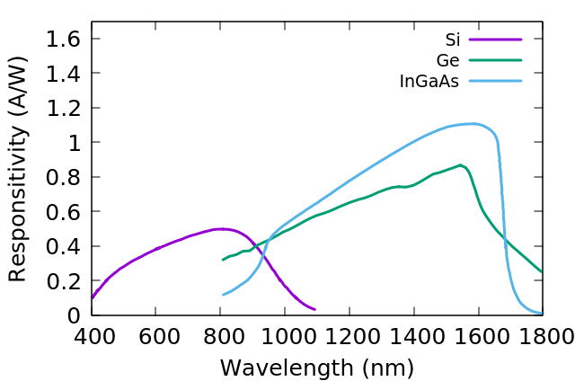
The biased photodiode works as an optical probe for an oscilloscope. It can be used to measure the time variation of optical signals. There is a large choice of photodiode for use as photodetector. There are different material, size, and packaging. The most used materials are silicone (Si ), germanium (Ge ), and Indium gallium arsenide (InGaAs ) in PIN or P–N junction structure. The different materials give band gaps that correspond to different absorption wavelengths. The figure shows responsivity at different wavelengths for common Si, Ge and InGaAs photodiodes. Si has good response in the visible wavelength range while InGaAs has been developed for the IR range. Optical fiber communication for example uses the 1550 nm range, where InGaAs photodiodes can be used as receivers.
Small area photodiodes are faster than large ones, because the junction has a capacitance which needs to be charge before signal is measured in the external circuit. The responsivity in Ampere power Watt (A/W) is independent of the size of the active are, but it is easier to capture light on a larger area. That is why we use small active area (few 100μ) for high speed (GHz) and large area (few mm) for high sensitivity applications. The photo induced current is measured as voltage drop across a termination resistor. A low impedance (50 ohm) gives the highest speed but less voltage swing than high impedance (1M). With low impedance termination, at both ends of the cable the total impedance is dominated by the pure resistive value and parasitic capacitance and inductance has less effect.
Small area photodiodes are faster than large ones. That is because the junction has a capacitance which needs to be charge before signal is measured in the external circuit. The capacitance grow with size (C=εA/d, A is the area and d the separation). The responsivity in Ampere per Watt (A/W) is independent of the size of the active area, but it is easier to capture light on a larger area. That is why we use small active area (few 100μ) for high speed (GHz) and large area (few mm) for high sensitivity applications. A large area also gives a larger linear range because the power is spread on a large area, so the saturation intensity is not reached as early as it would on a small area detector. The photo-induced current is measured as a voltage drop across a termination resistor. A low impedance (50 ohm) gives the highest speed, but with less voltage swing than with high impedance (1M) termination. With low impedance termination, at both ends of the cable the total impedance is dominated by the pure resistive value and parasitic capacitance and inductance has less effect.
Biased photodiode application
The BiasedPD is for measuring time varying optical signal with an oscilloscope. The example project below is prepared for a TO-can photodiode or a surface mount 0805 packaged photodiode. This gives access to a large number of photodiodes that allow you to optimize spectral and temporal response to your application. As bias voltage source a battery, or any DC power supply can be used.
Simplified schematic and function description
The photodiode (PD) is biased with a positive voltage on the cathode (reverse bias), so it is not conducting, but a field is created in the junction. The field cause accelerated drift of optically induced electron hole pairs to produce a fast current response.

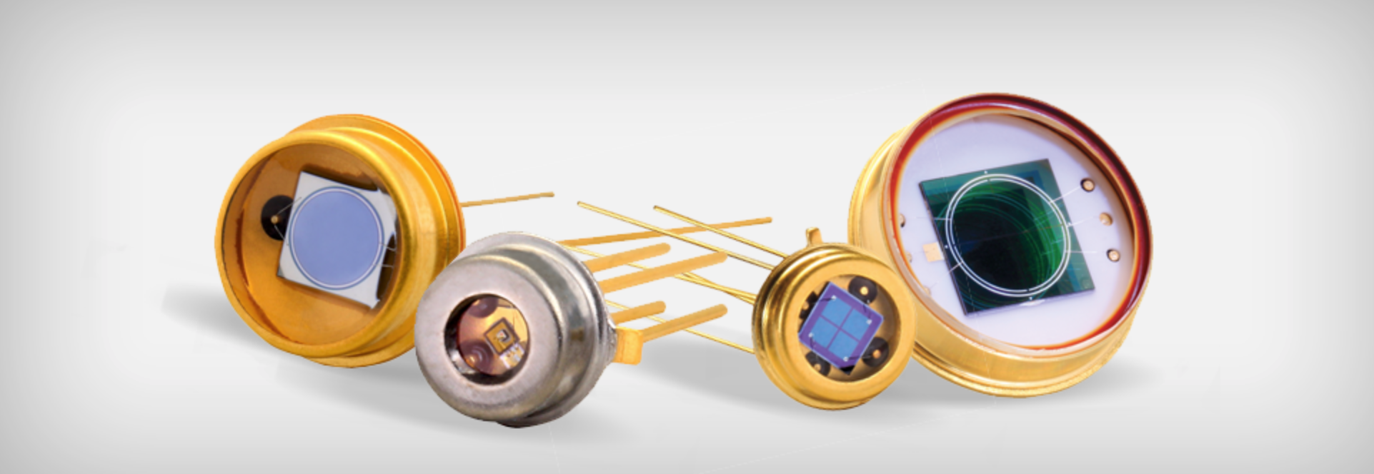
Electrically the biased PD acts as an optically controlled current source with compliance equal to the bias voltage (Vbias). The photocurrent can be detected as a voltage drop across a termination resistor and displayed on an oscilloscope. This type of detector is necessary for pulsed laser characterization, and in general as an optical probe for oscilloscopes to study time varying optical power in the 100ps to 10s range. Photodiodes come in different packages, most of which are based on TO- transistor through hole metal cases. With photodiodes finding their way into consumer goods, for example in remote control cheaper plastic packages have been developed. They look like a clear or black LED. The black over-molding is a spectral filter that blocks out the visible light and transmit only the near infrared used in remote control. Small form factor surface mount photodiodes are getting popular because they are compatible with the predominant electronics assembly process.
The price of a photodiode vary as much as the specifications with the high-end costing several thousand dollars and the cheaper selling at 10 cent.
What drives the price up is tailored spectral response and the size of the chip. In the other extreme there are very high speed (10-50GHz). These are fiber coupled and have RF coaxial output, so it is not just the photodiode adding to the price.
There exist ready integrated biased photodiode products on the market. They have a limited choice of integrated photodiodes and are quite expensive. In R&D work or budget development you might find yourself setting up a biasing arrangement. Not just to save money, but also to use the photodiode that best suite your needs in terms of spectral response, speed and active area.
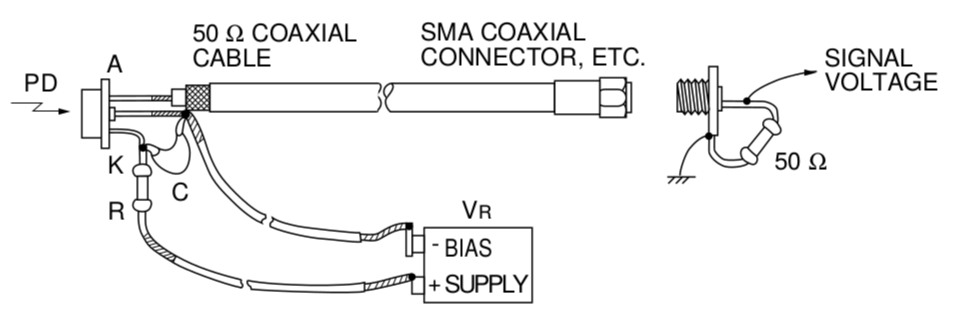
Source: HAMAMATSU PHOTONICS Application circuit examples of Si photodiode.
The figure shows an improvised biased photodetector arrangement. The core of a coaxial cable is soldered directly to the anode of the PD and the cathode is biased from a 9V battery through a resistor R. The capacitor is placed for transient decoupling. The coax shield is connected to the battery negative terminal and also to the PD package case ground. The output is detected on a 50 ohm terminated input, usually an oscilloscope.
This works. I can attest to that, because I have used it. It is not so easy to hold the PD in the setup. All that improvisation made me think, there must be as better way. That was when I started using open source EDA to design my own PCB’s. It is quite simple to design a circuit that does a lot.
Here I share a KiCad project for mounting and biasing a photodiode. It is shared as Open-source hardware (OSH, OSHW) and you are free to fabricate it from the Gerber files and BOM or use it as a basis for your tailored design.
Project files
The KiCad project files for the BiasedPD are in the list below for download. Here I will describe the circuit and the PCB layout and comment on some reasoning and choices.
The figure with the simplified schematic, tells that we at least need the photodiode and a bias voltage source. Incident optical signal produce a photocurrent going from cathode to anode. The photocurrent produce a voltage increase across a resistor connected to 0V. The voltage is the detector signal Vout.

The schematic has more components. It has a connector for the output signal (J1) and for connecting the bias voltage supply (J2). If you are new to EDA then it is good to know that the reference designator, like J1 is a unique reference to the component card in the EDA. That is, the address to the data that holds information about symbol, attributes like type of device, valur and footprint. The footprint is a definition of the mechanical component attachment featured which has to be placed on the PCB to mount the actual component. The schematic is an abstract representation that only have enough detail to communicate, calculate and simulate the behavior of the connection of components.
For the value attribute of the connectors we use a part number, that tell what connector we want to use. J1 is 112404 and a search will come up with the AMPHENOL RF BNC connector.

This connector is selected because most oscilloscopes have a BNC input connector, so most places you have an oscilloscope you already have BNC to BNC cables. The bias supply connector is TE Connectivity 1-2834016-2 2 Position Wire to Board Terminal Block.

This makes it easy to connect wires from any power supply. It can be a bench top power supply or for example a 9V battery, using a BATT CONNECTOR SNAP 9V 6" LEADS.

A battery is a low noise voltage source, but the schematic is prepared with supply filtering, so noise is not so critical. The photodiode responsivity is independent of the bias voltage, only the speed depends on the voltage. D1, R1, R2 and C1 are there to filter the supply. R1 and R2 are ferrite beads. They filter high frequency noise energy. They become resistive and dissipates the noise energy in the form of heat. The diode D1 together with the capacitor C1 is a rectifier that filters lower frequency noise. The diode also protects the PD from biasing the wrong way, which would drive current from anode to cathode and damage the PD. The component R3 is a current limiting resistor that protects the supply from accidental shorts (Imax = U / R= 9V / 27R = 333mA). The combination of R3 and C2 and C3 also acts a low pass filter for any supply noise. C3 in particular is meant as a decoupling capacitor, so that fast current transients for example from measurement of optical pulses are supplied by the capacitor. The schematic has two photodiodes D2 and D3. That is for alternative population, so only on should be fitted at a time. D2 adds a 0805 surface mount footprint for such surface mount photodiodes like Vishay TEMD7000X01. The other photodiode D3 adds a footprint for fitting more traditional three leg TO-can packages, like the TO46-3 of the MT03-023. With these photodiode footprints a large selection of Si, InGaAs and Ge can be used with the biasedPD PCB. R6, R5 and R4 are termination resistors. It would be sufficient to terminate with a resistor on the oscilloscope end of the BNC coaxial cable. The termination resistors on the PCB help to reduce ringing in the cable.

The PCB layout is quite simple, but it serves as a good example to highlight some considerations. We always need to consider; Signal integrity, power supply and mechanical design. The board has one high speed signal path from the PD anode to the BNC signal pin. This is kept short and has an unbroken GND return under it. The power supply will carry very low current os copper cross-section is not a concern. The wire connections to the supply connector J2 can pick up noise. There is filtering of the supply near the connector and the GND is split in two islands. There is a GND from the BNC shield and there is a negative return for the positive bias voltage. We want the to reference the negative supply to 0V GND but avoid ground-loop noise pick-up. This is done by only connecting the two with a thin track. The decoupling capacitor C3 is connected to the BNC GND, together with the termination resistors. This closes the high speed current loop, so current can flow from the capacitor positive through the PD and return to the capacitor negative through the termination resistor.
The mechanical design is based on mounting the detector on a standard optical post with a mounting bracket.

The BNC connector is placed centered and as near the mounting point as possible because the cable will exert force on the PCB.
The KiCad project files for the BiasedPD are in the list below for download.


| Description | File name | Download |
|---|---|---|
| BiasedPD KiCad bill of material (BOM) | KiCad_BOMfilled.csv | Download |
| BiasedPD KiCad Gerber files | BiasedPD_KiCad_production_files.zip | Download |
| KiCad Project, use unarchive project | BiasedPD_KiCad.zip | Download |